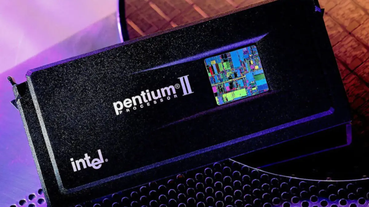
The 350 nanometer process is a level of semiconductor process technology that was reached in the 1995–1996 timeframe
The new stuff is 3nm

350 nm is massive and ancient relative to new processes, but the name of a new process stopped physically meaning anything a while ago. for instance, the 3 nm process smallest distance between traces is only 24 nm.
now the industry just names a new process when enough techniques for improving performance (without much actual size difference) exist.

The newest stuff out of Taiwan is 1.6nm.

Soon they’ll be able to run Doom.

Doom was actually a little before the 350nm era. Doom was like 386 and 486 timeframe; the first Pentium machines were being made when it was released, whereas 350nm was the Pentium Pro. So if they’re working on 350nm, they’re already ahead of Doom level hardware, hopefully.

Russia: Sanctions aren’t doing shit, we’re actually better off without the outside world
Also Russia: Hey never mind about the toilets, let me show you how we’ve mastered Nintendo 64 technology

masteredstarted working with
Yes, you are correct, that’s a very relevant correction. “Soon,” they say.

Chips is going in missiles and tanks arn’t leading edge. They kill just as effectively.

GMLRS: And I took that personally


