The 8-bit home computers of yore that we all know and love, without exception as far as we are aware, had an off the shelf microprocessor at heart. In 1983 you were either in the Z80 camp or the 65…
Sounds a bit like a repogrammable ROM (which is no longer ROM in that case, ROM=Read Only Memory). Kinda what FPGA does, if I’m not mistaken (and what you were referring to, right?).
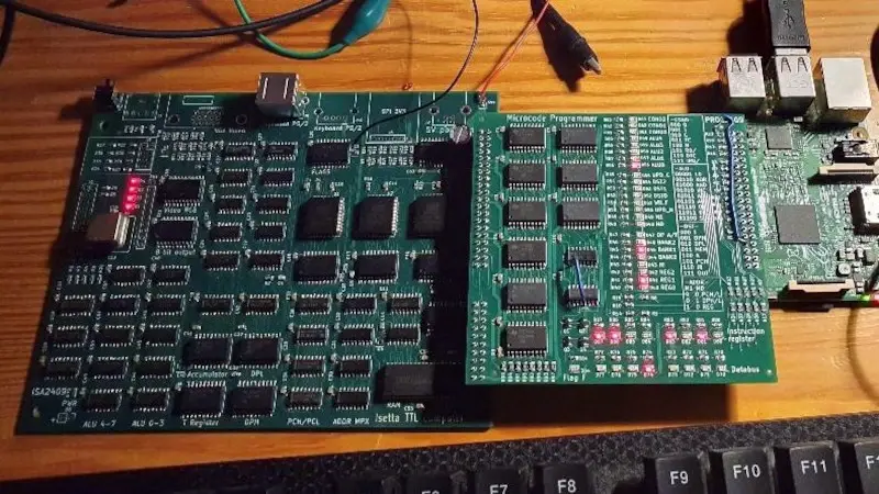
If you take a look at the die you’ll find what is in effect a ROM on board, a look-up table defining what each instruction does. A machine with said capability can change this ROM, and not merely emulate a different instruction set, but be that instruction set.
I am not good in that hardware emu branch but my guess is that they pick something that can drive and matches original clock speed as the old programmable rom was no longer produced. (the antique people would buy old broken ones and rip parts off them or try to restore them.)
ROMs back then got erased by UV light, EPROM. EEPROMs are a bit newer (though still ancient) and can be erased electronically, nowadays it’s a very sane idea to just throw flash storage at the problem. I think you can get modern replacement for pretty much any ancient form factor.
The way those things are used are basically big logic tables: Instead of using a bunch of logic gates, you store the output that’s expected given a certain input. Completely ancient technique, the limiting factor is storage space and sensibility – storing all addition results of two 32 bit numbers uses a lot more transistors than a 32-bit adder, but if what you want to put in there isn’t a thing that can be implemented few standard TTL components throwing storage at the problem makes sense even if you never plan to reprogram it because burning a custom set of transistors onto silicon is expensive.
Thanks for letting me know about this logic table thing, that explains my question when younger why some old computers had massive array of same components put together.
ps. my first computer was a 80286 knock off. By the time I get to high school(basically 80386 era) that have a computer tech club where member bring their old computer parts to share, they are mostly no longer functional. I basically donated my old 80286’s 20MB hard drive for tear down and that’s first time me and other member see what it looks like inside a hard drive.
It’s an legit 8-bit CPU implemented with TTL chips, what makes it a different beast than what they did back in the days is that its microcoding isn’t kneecapped. It would absolutely have been possible back in the days to build exactly such a thing, even from precisely those components. At least the TTL part, that is, I bet there’s wibbles around VGA etc. And because I already hear the detractors yes, 8-bit CPUs were microcoded: They decoded single external instructions into a stream of “load from memory, fetch from register so and so, switch on the ALU, put what’s in the ALU output somewhere”. They kept it as simple as possible and it wasn’t reprogrammable but that stuff there, that’s microcode.
Implementing CPUs in TTL chips also isn’t a new idea, that’s how early minicomputers were made (later on they got some specialised chips). And those things also used ROMs for their microcode. So you could say that this is a minicomputer capable of pretending to be different 8-bit microcomputers.
FPGAs are a completely different technology, those allow you to arrange logic in a (more or less) arbitrary topology. That is, looking at that board with all those TTL chips, it’d be the equivalent of being able to re-route all the board traces as you please.

Sounds a bit like a repogrammable ROM (which is no longer ROM in that case, ROM=Read Only Memory). Kinda what FPGA does, if I’m not mistaken (and what you were referring to, right?).
not necessary FPGA but can be re-writable: see
https://electronics.stackexchange.com/questions/243712/eeprom-is-a-read-only-memory-so-why-can-i-write-to-it
I am not good in that hardware emu branch but my guess is that they pick something that can drive and matches original clock speed as the old programmable rom was no longer produced. (the antique people would buy old broken ones and rip parts off them or try to restore them.)
ROMs back then got erased by UV light, EPROM. EEPROMs are a bit newer (though still ancient) and can be erased electronically, nowadays it’s a very sane idea to just throw flash storage at the problem. I think you can get modern replacement for pretty much any ancient form factor.
The way those things are used are basically big logic tables: Instead of using a bunch of logic gates, you store the output that’s expected given a certain input. Completely ancient technique, the limiting factor is storage space and sensibility – storing all addition results of two 32 bit numbers uses a lot more transistors than a 32-bit adder, but if what you want to put in there isn’t a thing that can be implemented few standard TTL components throwing storage at the problem makes sense even if you never plan to reprogram it because burning a custom set of transistors onto silicon is expensive.
Thanks for letting me know about this logic table thing, that explains my question when younger why some old computers had massive array of same components put together.
ps. my first computer was a 80286 knock off. By the time I get to high school(basically 80386 era) that have a computer tech club where member bring their old computer parts to share, they are mostly no longer functional. I basically donated my old 80286’s 20MB hard drive for tear down and that’s first time me and other member see what it looks like inside a hard drive.
Some more technical info.
It’s an legit 8-bit CPU implemented with TTL chips, what makes it a different beast than what they did back in the days is that its microcoding isn’t kneecapped. It would absolutely have been possible back in the days to build exactly such a thing, even from precisely those components. At least the TTL part, that is, I bet there’s wibbles around VGA etc. And because I already hear the detractors yes, 8-bit CPUs were microcoded: They decoded single external instructions into a stream of “load from memory, fetch from register so and so, switch on the ALU, put what’s in the ALU output somewhere”. They kept it as simple as possible and it wasn’t reprogrammable but that stuff there, that’s microcode.
Implementing CPUs in TTL chips also isn’t a new idea, that’s how early minicomputers were made (later on they got some specialised chips). And those things also used ROMs for their microcode. So you could say that this is a minicomputer capable of pretending to be different 8-bit microcomputers.
FPGAs are a completely different technology, those allow you to arrange logic in a (more or less) arbitrary topology. That is, looking at that board with all those TTL chips, it’d be the equivalent of being able to re-route all the board traces as you please.